- The experts' corner
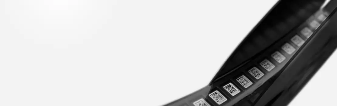
How to test the electrical continuity on a BGA...
...without a specific test socket?
The program
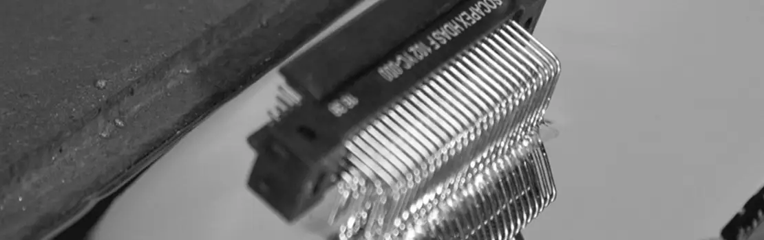
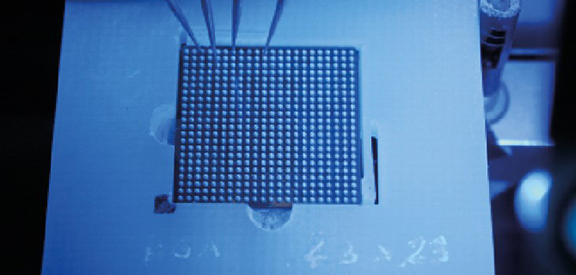
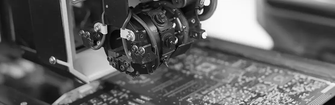
We do not often attempt to functionally test this type of complex component during broker purchases, it is generally a question of verifying that the ball is well connected to the chip by measuring the ESD protection diodes present on most of the I/O of the component. In practice, a current of the order of 10 to 100μA is injected, and the voltage across this diode is measured. The aim of these measurements is to check that all the components behave in a homogeneous way or, in the best case, to check that their behaviour is similar to a reference component. The programming then amounts to making the moving probe tester believe that it is measuring diodes on a PCB when in fact it is measuring the diode voltage between the I/O and GND of the component.
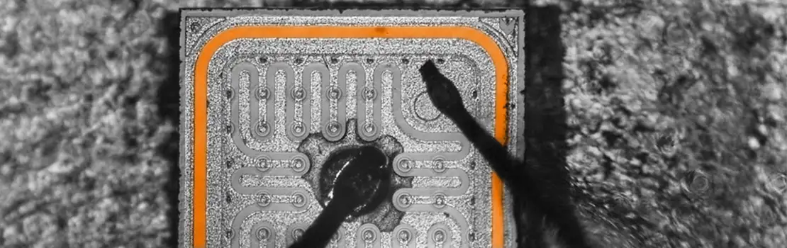
From that mechanical plan, we describe all the coordinates of the balls to which a probe will be connected, and then we describe, for each protection diode to be measured, to which ball positions it corresponds. In the same way, it is possible to check not diodes, but simple continuities, between all the balls connected to the GND and between all the balls of the different Vcc.
And in practice...
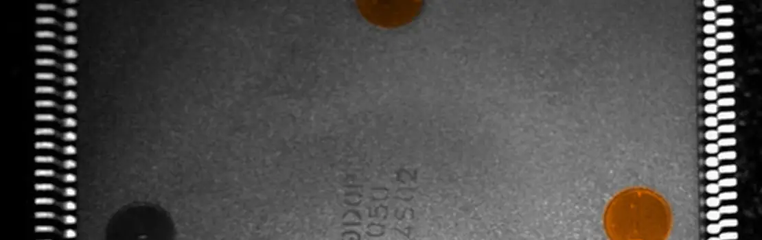
The main unknown was whether the touch points would deform the balls. In practice, there was a slight mark at the contact point, but it was still within the acceptable limits of ball deformation. In addition, the algorithms of the moving probe testers allow for only one GND contact to be made for all the different diode measurements, without having to hit a GND ball again for each measurement. It is also possible to set the approach and contact speeds on the balls to ensure that they are as gentle as possible.
This results in highly repeatable measurements, without degrading the components, with a measurement rate of several balls per second (depending on the number of probes available on the tester). The test is of course only carried out at room temperature, but it has the advantage of covering the entire I/O of the component with very low costs and, above all, very short tooling times.
Contact
Offers tailored to the different stages of your project
DevSolutions
Electronic product design consulting
FabSolutions
Electronic component quality control
 Best seller
ObSolutions
Electronic component obsolescence – Advice and strategic choices